In my second-last university co-op work term, January-April 1989, I finally succeeded at getting a job in the hardware field, namely in Product Integrity at Bell-Northern Research. This is where they did the "shake and bake" and other integrity tests on the carrier-grade hardware that Northern Telecom (now Nortel Networks) makes.
A fringe benefit was that interesting bits of hardware would sometimes get thrown out, and I was always ready to take those apart to get components for my own projects. I found that by the end of the semester, I had almost all the parts needed to build a small computer. Back in those days, building your own computer "from scratch" was a sort of rite of passage for a computer engineer. Nowadays it's much harder because the hardware components have become so high-tech and nothing counts as a "computer" unless it runs at least Linux and speaks TCP/IP. Of course it's all relative. Fifteen years before I did my project, "from scratch" might have meant wiring up your own CPU from small-scale integrated circuits, and ten years before that you'd probably have made it out of individual transistors!
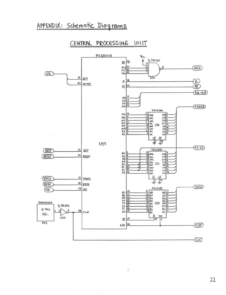
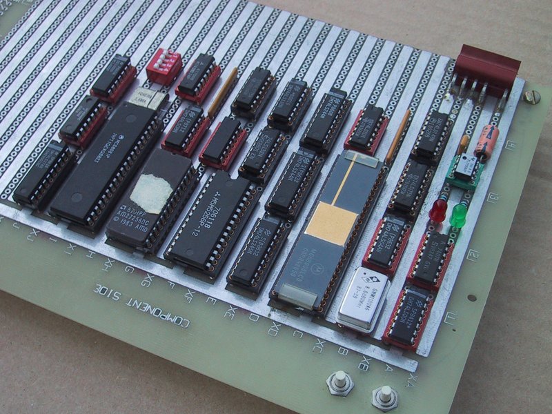
Anyway, my particular computer was built on a small wirewrap board. It had a MC68008 processor, which was a 68000 in a small package with an 8-bit external data bus and 20-bit external address bus. The 68000 series (68000/010/020) was in all the cool computers back then, Sun and Apollo workstations, Amiga, Atari, Macintosh computers and so forth. It had a very nice architecture that was a pleasure to program in assembly language. By comparison, the 80286 processor then used in most PCs was an ugly hack, and the PCs ran MS-DOS 3.3. The 386 was just coming out. Nobody could foresee that ten years later we hackers would all be running Unix on a descendant of that CPU, nobody would program in assembly language any more, and the 68000, the VAX and the other nice instruction set architectures of the day would be extinct.
Having designed and built the computer, and written a machine language monitor for it (debugging the monitor by running it natively on the Amiga at first, downloading it into RAM on the board using an earlier version of itself later), I figured I would see if I could get away with documenting it as a work-term report. It had nothing whatsoever to do with my actual job, but I wrote the report with the appropriate slant and not only got away with it but even got a minor award for it.
I'm having a nostalgia moment, and if this interests nobody else it's still worth putting up just for my own enjoyment. I used a very high-tech procedure to resurrect the report: I did a strings on the old Amiga Word Perfect document, and then hand-converted the result to HTML in vi. It follows below. At the end are scans of my schematic pages, and the source code for the monitor.
The MC68008 microprocessor is introduced. An overview of the computer system is given, then the design of the system is described in detail. Several aspects of future expandability are discussed. Finally, practical applications of the completed system are investigated.
It is concluded that the MC68008 can be used to build a small eight bit computer with an unusually powerful instruction set. It is found that the design presented here can be easily expanded. It is further concluded that this design is not suitable as a general purpose computer, but would be suitable as an educational computer system or a dedicated controller.
It is recommended that the design be enhanced by using programmable logic technology to lower the chip count, and by adding a dynamic RAM controller. It is further recommended that the cost effectiveness of the present system for educational or control applications be investigated.
The design in this report is expandable without additional circuitry to 64K bytes of EPROM storage, and can reasonably be expanded up to 128K of static RAM storage. With the address decoding and interrupt handling circuitry provided, the processor's entire addressing space and interrupt facilities can be exploited by memory and I/O devices.
The design uses considerably fewer parts and about half the board space of a comparable system available from Motorola. It provides similar functionality, however. This is due to newer components being used, and only an eight bit data bus being needed.
A computer of the scale presented here is not suitable for general purpose computing. However, it is suitable for educational applications, and embedded control.
The suitability of this design as a dedicated, embedded controller should be investigated, and a comparison done between performance and circuit simplicity of this system and a comparable one based on a microcontroller.
This system should be investigated as a cost effective alternative to the MC68000 Educational Computer Board available from Motorola.
A dynamic RAM system should be designed for this board, to facilitate memory expansion beyond 128K bytes.
Soon after the MC68000 was introduced, it was followed by the MC68008. This processor is packaged as an 8 processor, but is software compatible with the MC68000 and the only major 8-bit processor with a 32-bit internal architecture. This makes it uniquely suitable for use in small systems where 16/32-bit performance is not required, but the convenience of a 32-bit instruction set is desirable.
This report presents a design for a minimal computer system using the MC68008, exploiting the unique features of the MC68008 to create a small (23 chip) computer which nevertheless executes a full 32-bit instruction set and is completely software compatible with 16-bit 68000 systems.
In the following sections, the design of the system is presented and discussed in detail. The system has been designed to be easily expandable, and this is also discussed. Finally, some applications of this project are suggested.
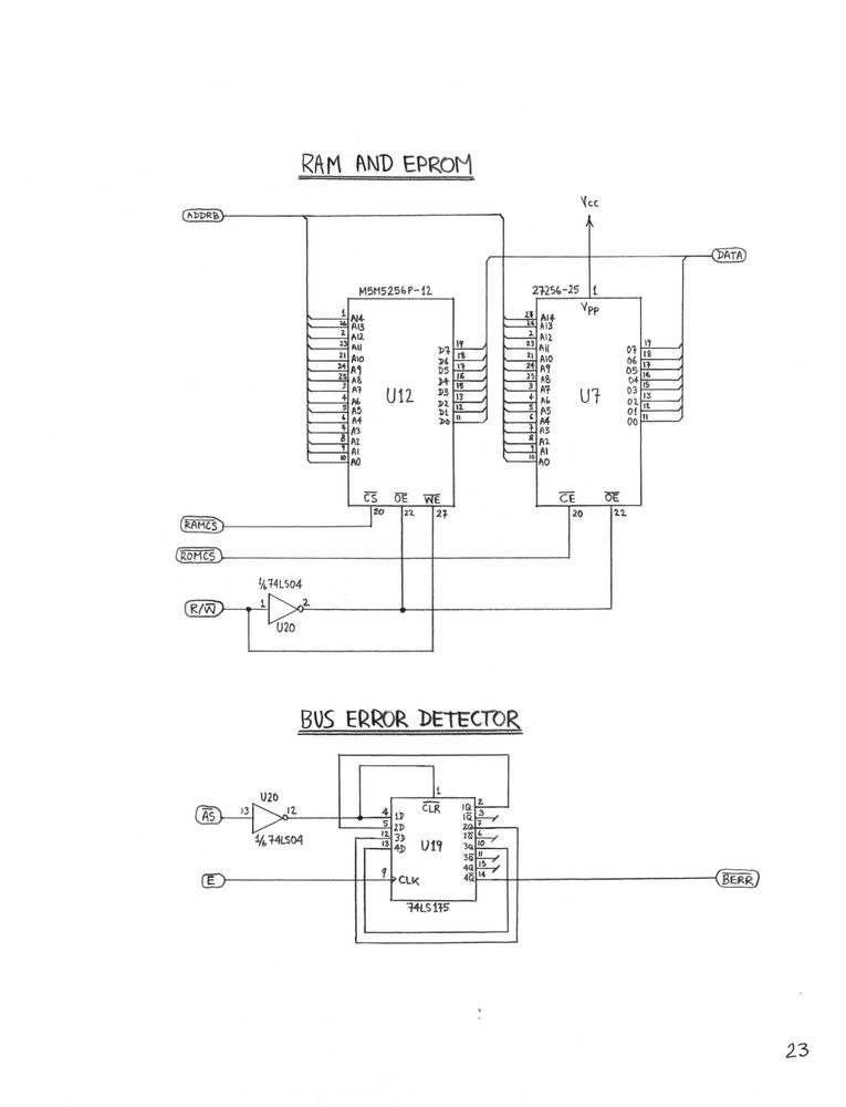
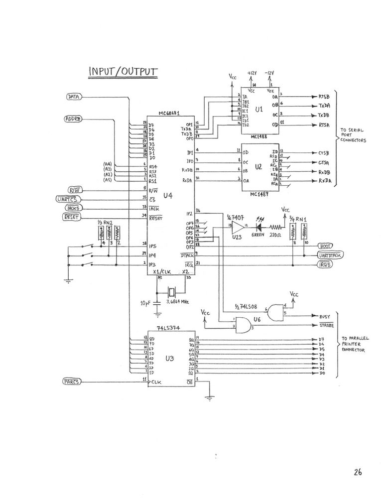
The serial I/O, timer, handshake lines for the parallel printer port, and several other control functions are all provided by a MC68681 DUART (Dual Universal Asynchronous Receiver/Transmitter). Memory is provided in the form of one 32K x 8 static RAM, and one 32K x 8 EPROM.
Two pushbuttons and two status lights are provided. The pushbuttons are used to reset the system, and to generate a non-maskable interrupt to the processor. One of the lights indicates when the processor is halted, while the other is user programmable.
The data bus and the low-order 16 address bits, which are passed to several other devices in the system, are buffered. 74LS244 bus drivers are used for the address lines. They are always enabled, since the processor is the only bus master in the system. The data bus is buffered by a 74LS245 bus transceiver, which is directly controlled from the R/W- and DS- outputs from the processor.
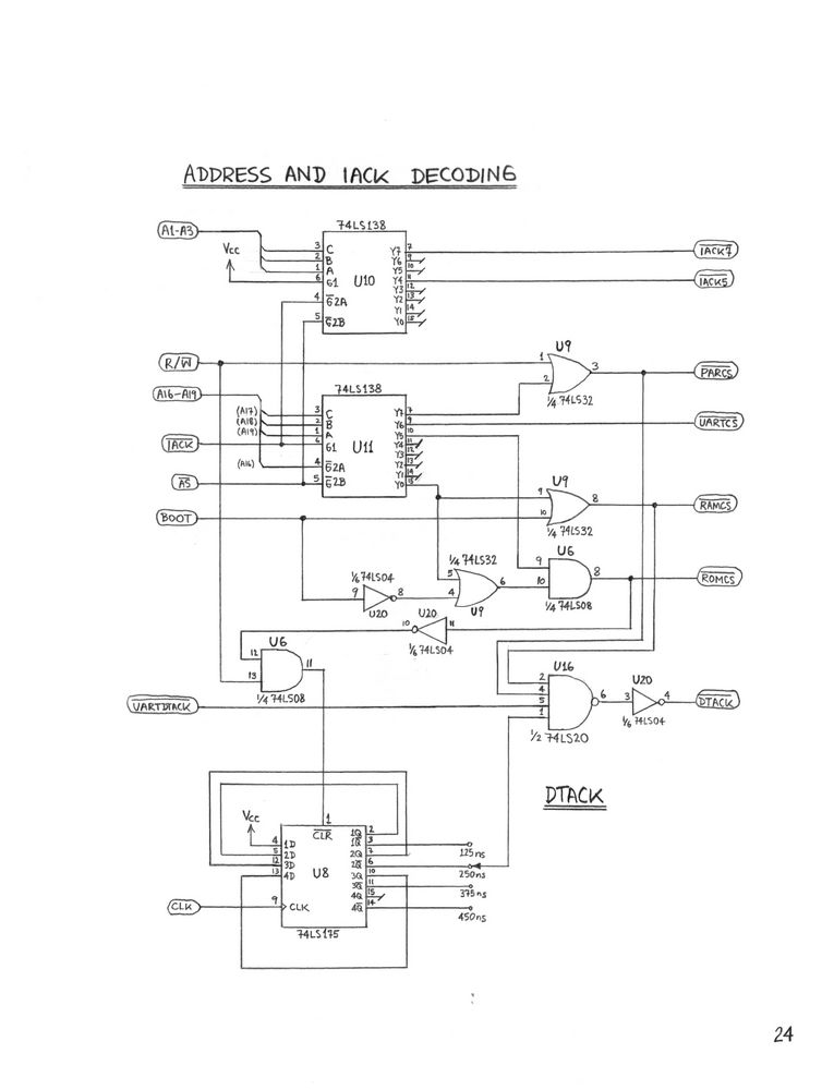
The FC0-FC2 outputs on the processor indicate the type of memory access which the processor is currently performing. Since this system does not use memory protection, the only function code which needs to be decoded is the one indicating an interrupt acknowledge (IACK) cycle. For IACK cycles, FC0-FC2 are all high. This is decoded by a NAND gate, producing the IACK- signal.
| $00000 - $1FFFF | RAM (ROM at powerup) |
| $20000 - $3FFFF | Not used |
| $40000 - $5FFFF | Not used |
| $60000 - $7FFFF | Not used |
| $80000 - $9FFFF | Not used |
| $A0000 - $BFFFF | ROM |
| $C0000 - $DFFFF | DUART |
| $E0000 - $FFFFF | Parallel output port |
Since none of the above devices occupy more than 32K of address space, the addresses are further decoded by feeding A16 into a spare enable input on the decoder, thus disabling the upper 64K of each bank.
On the MC68008, a memory address is only valid when AS is asserted, and the bus cycle is not an IACK cycle. Therefore, the AS- and IACK- signals from the processor block are fed into an active low and active high input on the decoder, respectively.
As can be seen on the schematic, the parallel port select signal is further qualified by the R/W- line. A read cycle on the parallel port register will not have any effect, and eventually a bus error timeout will occur.
The BOOT input to the address decoder is an active high signal, indicating that the processor is just starting up after a reset. This requires that it be able to fetch its program counter and initial stack pointer at address zero, where RAM is normally mapped. Thus, additional decoding is provided which maps the ROM into the RAM's address space, and disables the RAM, when BOOT is high. The BOOT signal is obtained from one of the DUART outputs. The DUART sets the signal when it is reset, and the processor resets it after the code in the ROM gains control.
The outputs from the address decoding circuitry are the signals PARCS-, UARTCS-, ROMCS-, and RAMCS-. They enable the parallel output port, the DUART, the ROM, and the RAM, respectively.
There are four addressable devices in the system. Of these, only the DUART has a DTACK- output. This enters the DTACK block as UARTDTACK-, and is combined with the other DTACK- signals.
The EPROM, being an inherently slow device, has the most elaborate DTACK- generator in the system. The R/W- and UARTCS- signals are combined by an inverter and an AND gate, producing a high on the CLR- input of the 74LS175 quad flip-flop when the EPROM is selected for reading. The quad flip-flop is connected as a shift register, and when when its CLR- input goes high, it begins to clock logic 1's into itself. After one clock cycle (125 ns), the first flip-flop is set. 125 ns later, the second flip flop is set, and so on until the last one is set after 450 ns. Now one of the Q- outputs can be used as an EPROM DTACK- signal. In this design, 2Q- is used, which gives a 250 ns DTACK delay, corresponding to the access time of the EPROM used. When DTACK- reaches the processor, it negates AS-, which deselects the EPROM. This causes CLR- to the 74LS175 to go low again, and the circuit is reset to its initial state.
The RAM and the parallel output register are fast enough for "no wait state" operation. This means that they will be finished responding by the first time the processor tests DTACK-, and thus there is no need to delay DTACK- at all. The select inputs for the RAM and parallel output register are used directly as the corresponding DTACK- signals.
The four DTACK- signals are combined by a NAND gate and an inverter, then sent to the processor. Note that no DTACK- will be produced for any of the following invalid accesses:
The clock input of the 74LS374 is connected to the PARCS- output from the address decoder. This causes data from the data bus to be copied into the register on the rising edge of PARCS-, that is, when the processor deasserts AS-. The outputs of the 74LS374 are always enabled, and used to drive a parallel printer.
Two handshake signals are also required to communicate with the printer. These are STROBE- and BUSY. STROBE- is asserted briefly by the computer to signal that a data byte is available, and BUSY is asserted by the printer until it is ready for a byte again. These functions are provided using two of the general purpose input/output pins on the DUART.
The DUART itself connects directly to the MC68008 bus. The only feature worth noting is that address lines A1-A4, rather than A0-A3, have been used for the DUART register select inputs. This was done so the registers of the DUART are accessible at consecutive odd addresses, as they would be if the DUART was connected to a 16-bit MC68000. This allows driver software designed for 16-bit systems to be used unmodified.
As seen in the schematic, the three unused general purpose inputs on the DUART have been connected to DIP switches. These are readable by software, and are presently used to select the port and baud rate to be used to communicate with the terminal.
A general purpose output is used to control the user definable status light. Since the output does not have enough drive capability to drive a LED, one section of a 7407 high current driver is used.
Another output on the DUART is used for the BOOT signal to the address decoder. After a reset, the BOOT signal is asserted by the DUART, as it sets all outputs to logic high. This also causes the LED to be turned off. When the processor has read its program counter and stack pointer from the ROM, it deasserts the BOOT signal.
Finally, the two sets of serial data and flow control lines are buffered through a MC1488 RS-232 driver, and a MC1489 receiver. Note that the STROBE- and BUSY lines to the parallel port are also buffered through a pair of spare gates. This means that electrostatic discharge, short circuits, or other trouble at the I/O connectors is less likely to damage the DUART than to damage an inexpensive buffer chip.
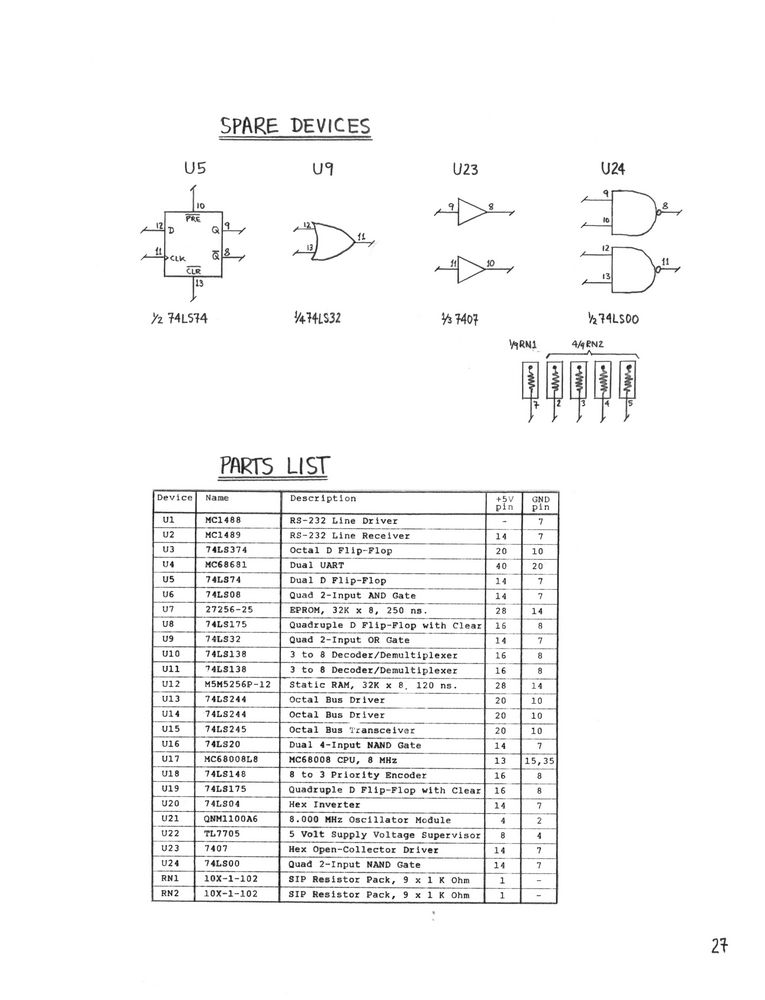
As shown on page 25, a 74LS148 priority encoder is used to generate the interrupt request level. Only part of the encoder functionality is used. Inputs are provided for level 2, 5, and 7 interrupts. Of these, the level 2 input is not presently used, and reserved for future expansion. The level 5 input is used by the DUART. Both need pullup resistors.
The level 7 interrupt is generated by a pushbutton. The pushbutton signal is first debounced by a NAND latch, then used to clock a logic one into a D flip-flop. This causes the flip-flop to be set whenever the pushbutton is pressed.
When the flip-flop is set, it asserts the level 7 interrupt to the processor. This is the non-maskable interrupt. When the processor accepts the interrupt, a level 7 IACK- signal is received from the IACK- decoder. This causes the flip-flop to be reset, and the interrupt request to be removed. As well, it causes the VPA- signal on the processor to be asserted, to indicate that no interrupt vector number is being supplied and the processor should treat this as an "auto vectored" interrupt.
Finally, the IACK- decoder can be seen near the address decoding block on page 24. It decodes the interrupt level supplied by the processor on its low-order address lines during an IACK- cycle, and produces the appropriate IACK- signal. The level 5 IACK- is fed to the DUART, while the level 7 IACK- is fed to the pushbutton circuitry just discussed. All other IACK- outputs have no present function.
To reset an MC68000 series processor, both the HALT- and RESET- lines on the processor must be pulled low. This is accomplished using two sections of a 7407 open collector driver. The HALT- and RESET- signals also have output functions. Specifically, the processor will assert HALT- when it has ceased to operate because of a severe bus error, and this event is signaled by a red LED indicator. The processor will assert RESET- when instructed to do so from software, and this can be used to reset certain I/O devices, in this case, the DUART.
When AS- goes low, the CLR- input of the shift register is deasserted, and logic ones are clocked into the shift register. If AS- remains asserted for four cycles of the 800 KHz E clock, the logic one will have propagated through the fourth flip-flop, and 4Q- will go low. This will terminate the bus cycle by asserting the BERR- input to the processor, causing a bus error exception.
This circuit times out when AS- remains asserted for more than approximately 4 x (1 / 800 KHz) = 5 microseconds. This is far longer than the response time of any device likely to be connected to the bus.
Presently, four of these 64K banks are not in use, permitting the addition of four I/O or memory devices without any change in address decoding. If any of these four additional devices were to require an entire 128K bank, rather than just the lower 64K, then address line A16 would have to be disconnected from the decoder, and the corresponding input tied to ground. This would not affect the decoding in any adverse way except to cause less of the unimplemented address space to give bus errors when accidentally accessed.
If even more banks were required, then a second 74LS138 device could be added, and its G2A- input tied to an inverted version of A16. This would decode the upper half of each 128K bank, thus fully decoding the MC68008 address space into sixteen 64K banks with only the addition of one 74LS138 and one inverter.
The RAM is currently implemented using a single 32K byte static RAM chip. Additional static RAM chips could be added by installing further sockets and a small amount of decoding of the A15 and A16 lines. It is suggested that the system only be expanded to 128K bytes using static RAM, as dynamic RAM becomes more cost effective beyond this point. This is because 256K bytes of dynamic RAM can be implemented, with present technology, as two 256K x 4 devices, taking up little more space than the present 32K x 8 static RAM chip. The remaining space would be devoted to a DRAM controller, which in total would take up less space than eight 32K x 8 static RAM devices.
To add interrupt devices beyond this point, a daisy chain technique would have to be used, to arbitrate IACK- signals among the interrupt requesting devices.
The difference in complexity between the Motorola board and the design presented here is primarily due to the fact that this design uses several parts not available when the Motorola board was designed, and requires less circuitry due to its use of an eight bit data bus.
With a monitor program similar in function to that provided with the Motorola board, this design could equally well be used in an educational context, at a potential savings in cost. Most of the required monitor program has been implemented.
It is therefore suggested that for those embedded control applications where program storage, RAM or I/O requirements exceed the capabilities of a traditional microcontroller, this design could be investigated instead. It offers easy expandability once the basic computer is in place, an unusually powerful instruction set for an eight bit machine, and a large address space not normally found in a microcontroller. Additionally, some of the circuit complexity of this design could be further reduced by employing a programmable logic device (PAL) in place of the present clutter of MSI devices. This would bring the chip count into the range traditionally expected for small embedded control systems.
Brown, Geoffrey and Harper, Kyle, 1984. MC68008 Minimum Configuration System. Motorola application note AN897.
Harper, Kyle, 1984. A Terminal Interface, Printer Interface, and Background Printing for an MC68000 based System using the MC68681 DUART. Motorola application note AN899.
Motorola, Inc., 1981. MC68000 Educational Computer Board. Motorola publication MEX68KECB.
Motorola, Inc., 1988. M68000 Family Reference Motorola publication FR68K/D.
Motorola, Inc., 1989. MC68000, MC68008, MC68010, MC68HC000 8-/16-/32-Bit Microprocessor User's Manual, 6th Edition. Motorola publication M68000UM/AD Rev 5.